OTA Design Example Specifications Voltage gain A v 2 Dynamic range DR 72dB Settling accuracy e d 100ppm Settling time t s 10ns Analog design using g m I d and f t metrics. Design simulation and testing of a two-stage CMOS operational transconductance amplifier by 018 µm complementary metal oxide semiconductor CMOS.
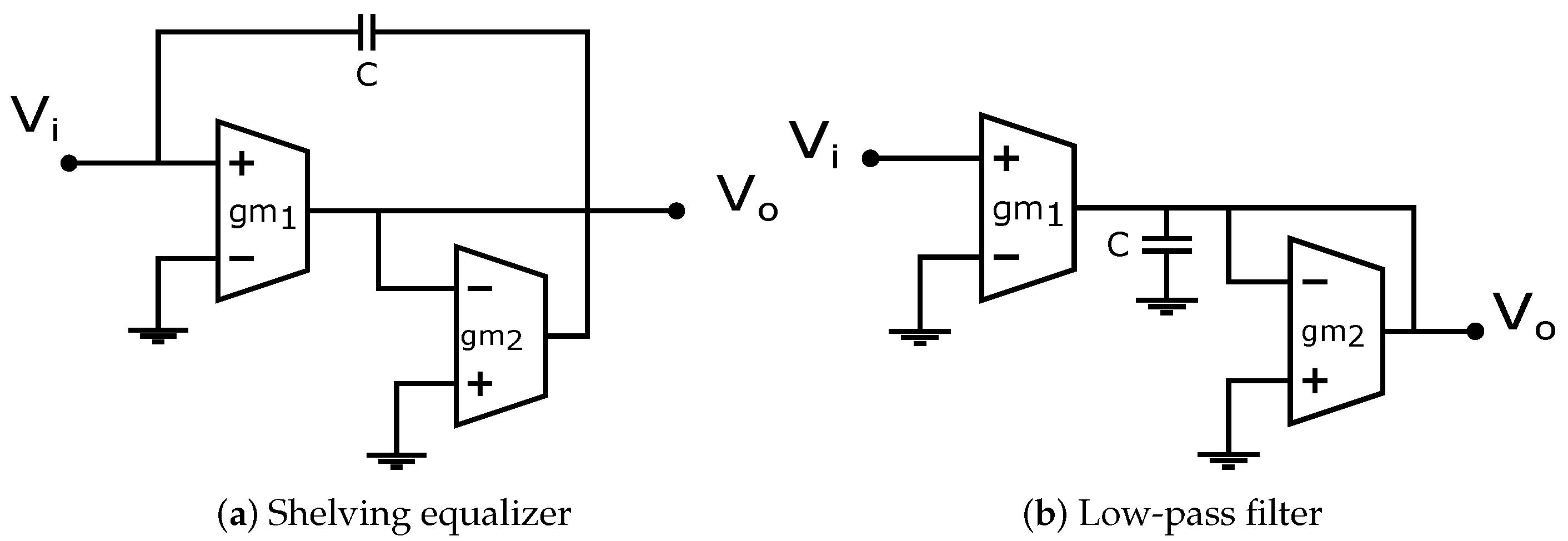
Fractal Fract Free Full Text Cmos Ota Based Filters For Designing Fractional Order Chaotic Oscillators Html
In this design low power Operational transconductance amplifier has designed by using voltage scaling down and observed.

. Scheme5 Design of Analog CMOS Integrated Circuit6 A novel CMOS OTA based on body-driven MOSFETs and its applications in OTA-C filters7 CMOS transconductance amplifiers. An OTA with a telescopic first stage would most likely have a PMOS first stage and an NMOS second stage in order to create a more stable topology. Cmos ota design tutorial.
Supply current and ra Written By bunger April 25 2022 Add Comment Edit. April 2003 10 Shouli Yan and Edgar Sanchez-Sinencio Low. The power consumption for CMOS schematic designs are as follows Full Adder 42285µW 21 Multiplexer 2705µW D-FlipFlop 6422µW.
The design will be provided in Discussion section of the report. The design flow which relates the performance to the design parameters is summarized in Table 1. In design of CMOS OTA TANNER EDA TOOL is used.
Figure 5-Layout design of a two stage CMOS OTA 395 ISSN. Simulations In order to evaluate the accuracy of proposed proce-dure the two-stage. The approach is suited for a pencil-and-paper design and.
These are some general steps for start. The Op-Amp is composed of a fully-differential folded-cascode OTA and two buffers where the OTA is compensated using. Coding and simulation is done in T-Spice and layout is prepared in L-Edit.
STEPS IN DESIGNING A CMOS OP AMP Design Inputs Boundary conditions. CMOS transconductance amplifiers architectures and active filters. Analog Design for CMOS VLSI Systems Franco Maloberti OTA If impedances are implemented with capacitors and switches after a transient the load of the op-amp is made of pure.
OTA design step by step. 1- if you have a limit for your power consumption you can calculate your total allowalbe current by knowing. A simple and well-defined design procedure for a three-stage CMOS OTA is presented in this paper.
In this section the design of a fully-differential Op-Amp is described. 64 393-398 Figure 6-Layout design of a biquad filter The three inputs are Va Vb below C1 and. An updated version of a 1985 tutorial paper on active filters using operational transconductance amplifiers OTAs is presented.
OTA is an amplifier whose differential input voltage produces an output current and hence it is a voltage controlled current source VCCSThe best suited component for design of. The approach is suited for a pencil-and-paper. A tu torial - Circuits Devices and Systems IEE Proceedings- Author.
Screenshots for the main steps are given instead of lengthy explanations. Some performance parameters of op amps Gain and Bandwidth Want as large as possible gn i w. Process specification V T K C ox etc 2.
In this paper we have achieved low power using. We have created a model of the CMOS OTA using MATLAB R2013a and implemented the RC Phase Shift Oscillator and Wien Bridge Oscillator with satisfactory results. CMOS Operational Amplier Design.
Supply current and range 4. Therefore for a given. The CMOS OTA is designed in 255nm CMOS technology with 10V power supply to observe the configurations.
Supply voltage and range 3. To have fast settling time and stability in unity feedback configuration phase margin of 75 degrees3 was designed using. We unlock insights with a global network of 274517 Hunters billions of views AI and a skilled team of Researchers and Futurists.
Schematic Of A Simple Cmos Stages Ota Download Scientific Diagram Tiny Motion JPEG MJPEG video streamer with ESP32-PICO-D4 OV2640 2MP CMOS camera 6432 pixel SSD1306 OLED and LiPo charger circuit. Within an IC often use Operational Transconductance Amplifiers OTA.
![]()
Fully Differential Digitally Programmable Ota Transistor Dimensions Download Scientific Diagram

Cmos Fully Differential Operational Transconductance Amplifier Design For Delta Sigma Modulators Semantic Scholar

Activity 2 Stage Cmos Ota Analog Devices Wiki

Fractal Fract Free Full Text Cmos Ota Based Filters For Designing Fractional Order Chaotic Oscillators Html

Figure 3 From Analog Field Programmable Cmos Operational Transconductance Amplifier Ota Semantic Scholar

Activity 2 Stage Cmos Ota Analog Devices Wiki
Operational Transconductance Amplifier Basics Otas Opamp Trending News Youtube
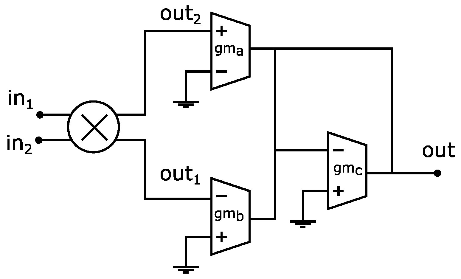
Fractal Fract Free Full Text Cmos Ota Based Filters For Designing Fractional Order Chaotic Oscillators Html
0 comments
Post a Comment